General Description
The RT4813 is a boost regulator designed to provide a minimum output voltage from a single-cell Li-Ion battery or two alkaline battery series, even when the battery voltage is below system minimum. Quiescent current in shutdown mode is less than 1µA, which maximizes battery life. In boost mode, output voltage regulator is guaranteed to supply 3.1A for maxium loading.
Performance Specification Summary
The boost conveter has an input voltage range from 1.8V to 5.5V, and the output voltage range is from 1.8V to 5.5V. It can operate in PFM mode and PWM mode in boost operation. And the power-on inrush current and current limit are implemented serval setting for difference application. The RT4813 is available in a UQFN-9L 2x2 (FC) package.
Table 1. RT4813 Evaluation Board Performance Specification Summary
|
Specification
|
Test Conditions
|
Min
|
Typ
|
Max
|
Unit
|
|
Input Voltage Range
|
|
1.8
|
--
|
5.5
|
V
|
|
Output Current
|
|
2.5
|
--
|
3.25
|
A
|
|
Default Output Voltage
|
Setting by FB pin
|
1.8
|
5
|
5.5
|
V
|
|
Operation Frequency
|
|
--
|
500
|
--
|
kHz
|
|
Output Ripple Voltage
|
VIN = 2.5V, VOUT = 5V, IOUT = 1A
|
--
|
60
|
--
|
mVp-p
|
|
Line Regulation
|
CCM, VIN = 2.7V to 4.5V, VOUT = 5V, IOUT = 0.5A
|
--
|
0.5
|
--
|
%
|
|
Load Regulation
|
CCM, VIN = 3.6V, VOUT = 5V, IOUT < 3.1A
|
--
|
0.5
|
--
|
%
|
|
Load Transient Response
|
VIN = 3.7V, VOUT = 5V, IOUT = 1.5A to 3A
|
-10
|
--
|
10
|
%
|
|
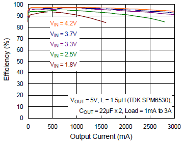
Maximum Efficiency
|
VIN = 1.8V to 4.2V, VOUT = 5V, IOUT = 0A to 3A
|
--
|
96
|
--
|
%
|
Power-up Procedure
Suggestion Required Equipments
- Connect input voltage (1.8V < VIN < 5.5V) to VIN pin.
- Setting output voltage by FB pin.(formula shown in below section)
- Setting BOOST pre-charge current and BOOST_LIMIT for power on inrush current. (setting 0x01 and 0x03 by I2C)
- To enable Boost converter by external EN pin.
- To connect an external load to output and verify the output voltage versus applied current.
Output Voltage Setting
The output voltage set by external feedback resistors expressed in the following equation.
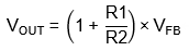
Where the reference voltage VFB is 0.5V (typ.)
The placement of the resistive divider should be as close as possible to the FB pin. For better output voltage accuracy, the divider resistors with ±1% tolerance or better should be used.
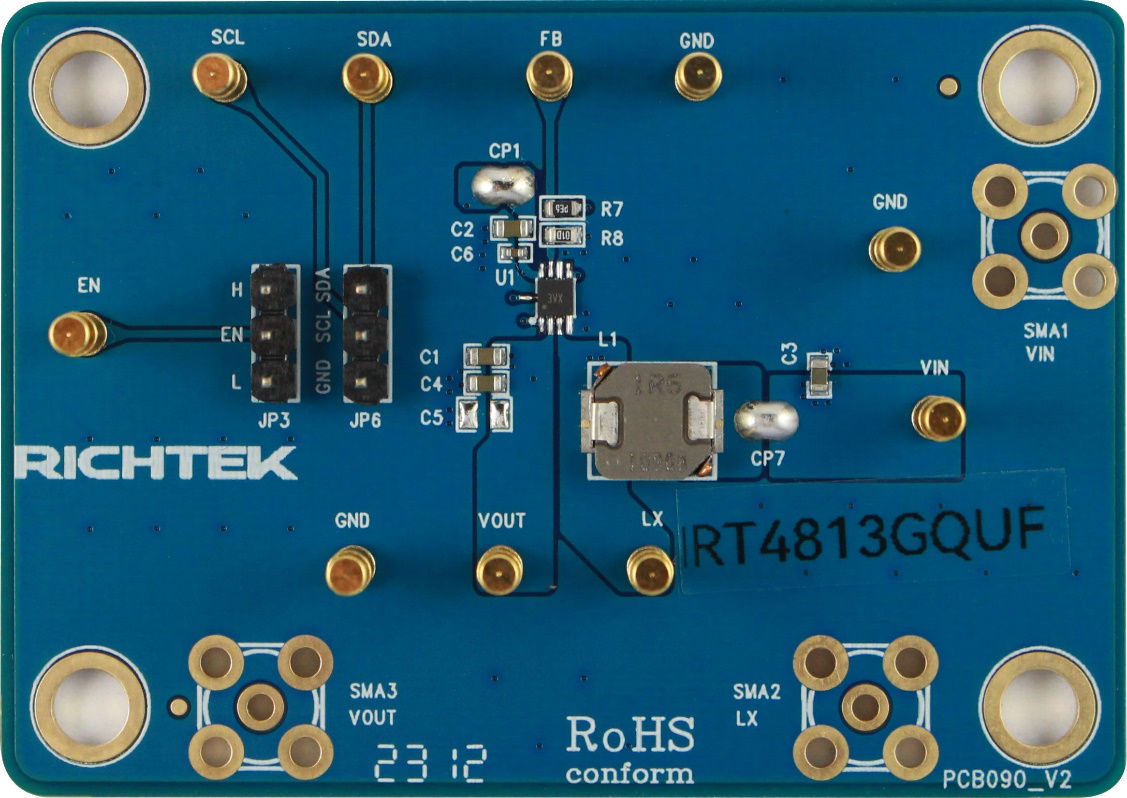
Detailed Description of Hardware
Headers Description and Placement
Carefully inspect all the components used in the EVB according to the following Bill of Materials table, and then make sure all the components are undamaged and correctly installed. If there is any missing or damaged component, which may occur during transportation, please contact our distributors or e-mail us at evb_service@richtek.com.
Test Points
The EVB is provided with the test points and pin names listed in the table below.
|
Test Point/
Pin Name
|
Function
|
|
VIN
|
Input voltage.
|
|
VOUT
|
Output voltage.
|
|
GND
|
Ground.
|
|
EN
|
Enable test point.
|
|
LX
|
Switch node test point.
|
|
SCL
|
I2C interface clock input.
|
|
SDA
|
I2C interface clock input.
|
|
FB
|
Voltage feedback.
|
|
PGND
|
Power ground.
|
Bill of Materials
|
|
VIN = 12V, VOUT = 5.0V, IOUT = 0.5A, fSW = 500kHz
|
|
|
Reference
|
Count
|
Part Number
|
Value
|
Description
|
Package
|
Manufacturer
|
|
U1
|
1
|
RT4813GQUF
|
RT4813GQUF
|
Step-Up
Converter
|
UQFN-9L 2x2 (FC)
|
RICHTEK
|
|
C1, C2,
C3, C4
|
4
|
JMK107BBJ226MA-T
|
22µF
|
22µF/6.3V/X5R
|
0603
|
TAIYO YUDEN
|
|
C6
|
1
|
0402X105K100CT
|
1µF
|
1µF/10V/X5R
|
0402
|
WALSIN
|
|
L1
|
1
|
SPM6530T-1R5M100
|
1.5µH
|
1.5µH/11A
|
6.5x7.1x3mm
|
TDK
|
|
R7
|
1
|
WR06X9093FTL
|
909k
|
909k
|
0603
|
WALSIN
|
|
R8
|
1
|
WR06X1003FTL
|
100k
|
100k
|
0603
|
WALSIN
|
|
|
|
|
|
|
|
|
|
Typical Applications
EVB Schematic Diagram
1. The capacitance values of the input and output capacitors will influence the input and output voltage ripple.
2. MLCC capacitors have degrading capacitance at DC bias voltage, and especially smaller size MLCC capacitors will have much lower capacitance.
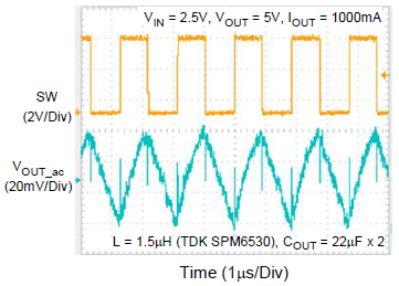
Measure Result
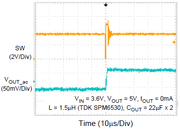
|
Output Ripple Measurement
|
Output Ripple Measurement
|
|
|
|
|
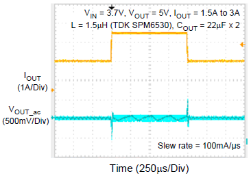
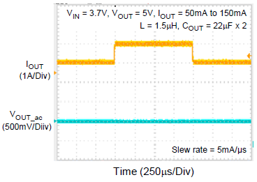
Load Transient
|
Load Transient
|
|
|
|
|
Efficiency vs. Output Current
|
|
|
|
|
Note: When measuring the input or output voltage ripple, care must be taken to avoid a long ground lead on the oscilloscope probe. Measure the output voltage ripple by touching the probe tip directly across the output capacitor.
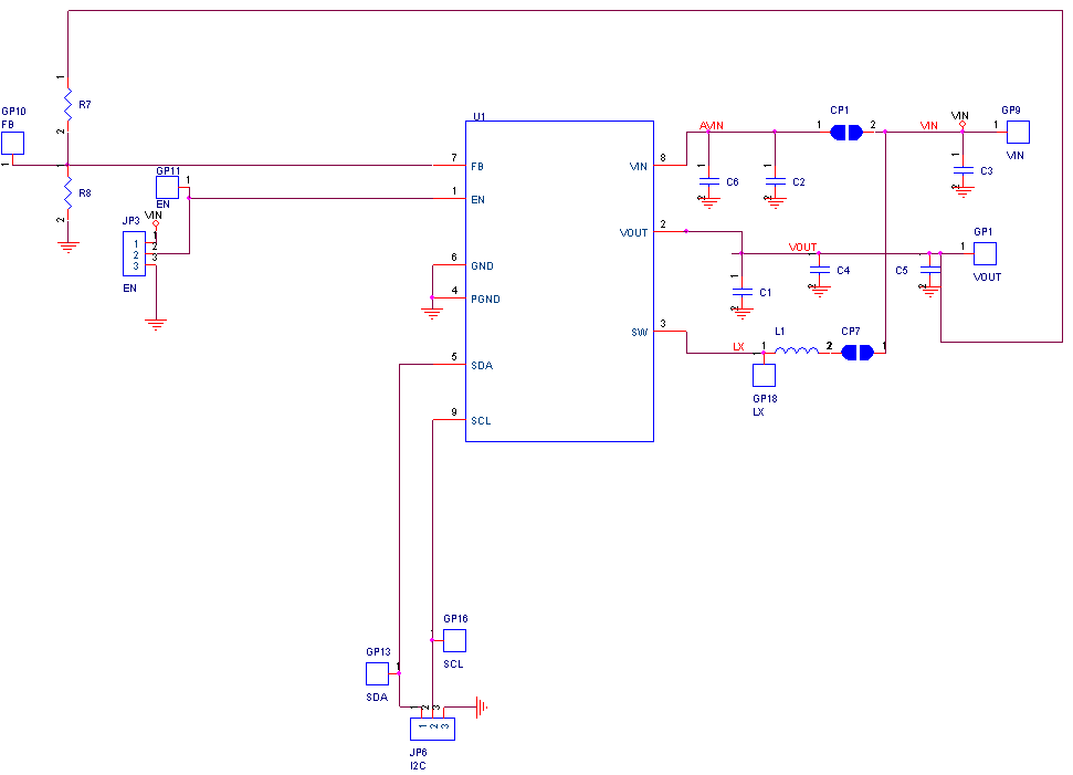
Evaluation Board Layout
Figure 1 to Figure 4 are RT4813GQUF Evaluation Board layout. This board size is 70mm x 50mm and is constructed on four-layer PCB, outer layers with 2 oz. Cu and inner layers with 1 oz. Cu.
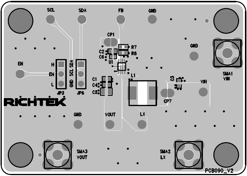
Figure 1. Top View (1st layer)

Figure 2. PCB Layout—Inner Side (2nd Layer)
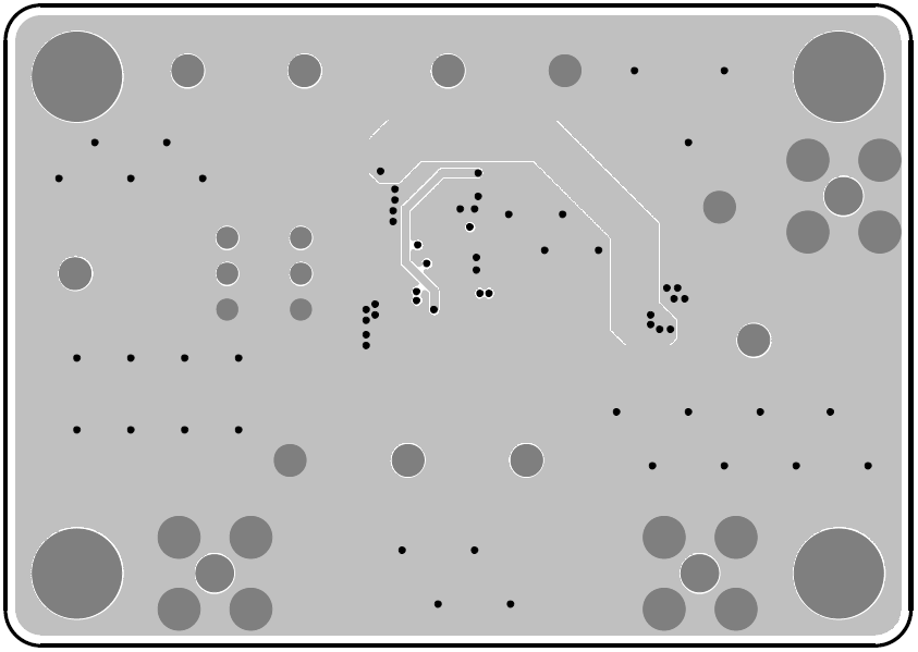
Figure 3. PCB Layout—Inner Side (3rd Layer)
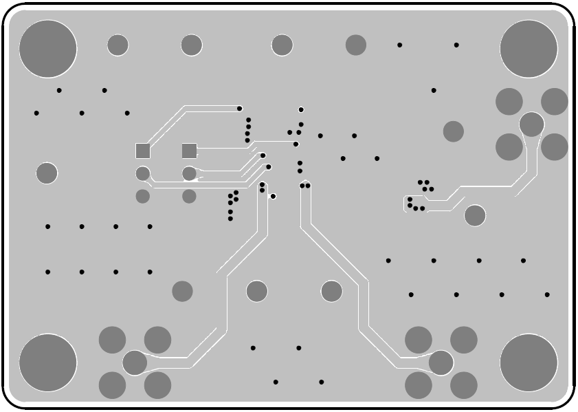
Figure 4. Bottom View (4th Layer)